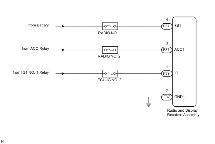
AUDIO AND VISUAL SYSTEM(for Radio and Display Type) Radio Receiver Power Source Circuit
DESCRIPTION
This is the power source circuit to operate the radio and display receiver assembly.
WIRING DIAGRAM
CAUTION / NOTICE / HINT
Note
Inspect the fuses for circuits related to this system before performing the following procedure.
PROCEDURE
-
CHECK HARNESS AND CONNECTOR (RADIO AND DISPLAY RECEIVER ASSEMBLY POWER SOURCE)
-
Disconnect the F37 and F39 radio and display receiver assembly connectors.
-
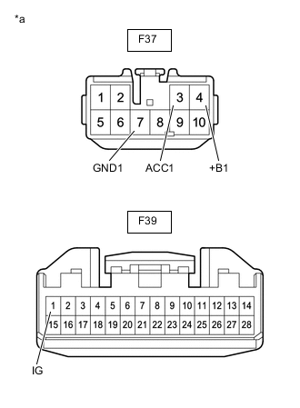
*a Front view of wire harness connector
(to Radio and Display Receiver Assembly)
Measure the resistance according to the value(s) in the table below.
Standard Resistance Tester Connection Condition Specified Condition F37-7 (GND1) - Body ground Always Below 1 Ω -
Measure the voltage according to the value(s) in the table below.
Standard Voltage Tester Connection Condition Specified Condition F37-4 (+B1) - F37-7 (GND1) Always 11 to 14 V F37-3 (ACC1) - F37-7 (GND1) Engine switch ACC 11 to 14 V F39-1 (IG) - F37-7 (GND1) Engine switch ON 11 to 14 V Result Proceed to OK NG
OK 
PROCEED TO NEXT SUSPECTED AREA SHOWN IN PROBLEM SYMPTOMS TABLE Click here
NG
REPAIR OR REPLACE HARNESS OR CONNECTOR
-