REAR SEAT ENTERTAINMENT SYSTEM Sound Signal Circuit between Video Terminal and Multi-display Controller
DESCRIPTION
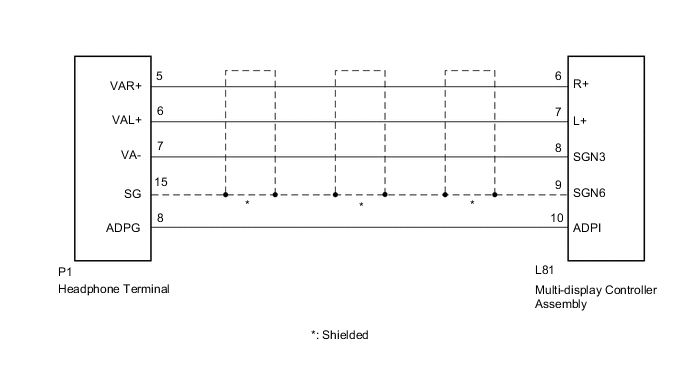
This is the sound signal circuit between the headphone terminal and multi-display controller sub-assembly.
WIRING DIAGRAM
PROCEDURE
-
CHECK HARNESS AND CONNECTOR (MULTI-DISPLAY CONTROLLER SUB-ASSEMBLY - HEADPHONE TERMINAL)
-
Disconnect the L81 multi-display controller sub-assembly connector.
-
Disconnect the P1 headphone terminal connector.
-
Measure the resistance according to the value(s) in the table below.
Standard Resistance Tester Connection Condition Specified Condition L81-6 (R+) - P1-5 (VAR+) Always Below 1 Ω L81-7 (L+) - P1-6 (VAL+) Always Below 1 Ω L81-8 (SGN3) - P1-7 (VA-) Always Below 1 Ω L81-9 (SGN6) - P1-15 (SG) Always Below 1 Ω L81-10 (ADPI) - P1-8 (ADPG) Always Below 1 Ω L81-6 (R+) - Body ground Always 10 kΩ or higher L81-7 (L+) - Body ground Always 10 kΩ or higher L81-8 (SGN3) - Body ground Always 10 kΩ or higher L81-9 (SGN6) - Body ground Always 10 kΩ or higher L81-10 (ADPI) - Body ground Always 10 kΩ or higher
OK 
PROCEED TO NEXT SUSPECTED AREA SHOWN IN PROBLEM SYMPTOMS TABLE Click here
NG
REPAIR OR REPLACE HARNESS OR CONNECTOR
-