THEFT DETERRENT SYSTEM (w/o Smart Entry and Start System) Ignition Switch Circuit
DESCRIPTION
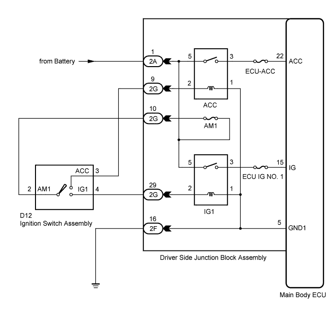
The main body ECU (driver side junction block assembly) determines the ignition switch position (OFF, ACC, ON) based on signals from the IG or ACC circuit.
WIRING DIAGRAM
INSPECTION PROCEDURE
PROCEDURE
-
READ VALUE USING GTS
-
Connect the GTS to the DLC3.
-
Turn the ignition switch to ON.
-
Turn the GTS on.
-
Select the items below in the Data List and read the display on the GTS.
Main Body Tester Display Measurement Item/Range Normal Condition Diagnostic Note IG SW Ignition switch ON signal/ON or OFF ON: Ignition switch ON
OFF: Ignition switch off
- ACC SW Ignition switch ACC signal/ON or OFF ON: Ignition switch ACC
OFF: Ignition switch off
- OK When the ignition switch is operated, the display changes as shown in the table.
NG 
CHECK HARNESS AND CONNECTOR (BATTERY - DRIVER SIDE JUNCTION BLOCK ASSEMBLY) Click here
OK 
PROCEED TO NEXT SUSPECTED AREA SHOWN IN PROBLEM SYMPTOMS TABLE Click here
-
-
CHECK HARNESS AND CONNECTOR (BATTERY - DRIVER SIDE JUNCTION BLOCK ASSEMBLY)
-
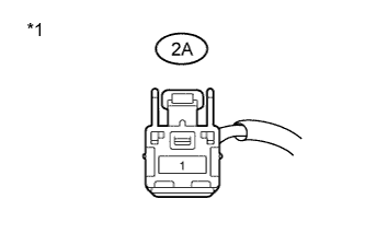
Text in Illustration *1 Front view of wire harness connector
(to Driver Side Junction Block Assembly)
Disconnect the 2A driver side junction block assembly connector.
-
Measure the voltage according to the value(s) in the table below.
Standard Voltage Tester Connection Condition Specified Condition 2A-1 - Body ground Ignition switch ON 11 to 14 V
NG 
REPAIR OR REPLACE HARNESS OR CONNECTOR
OK 
-
-
INSPECT IGNITION SWITCH ASSEMBLY
-
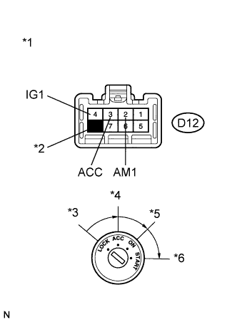
Text in Illustration *1 Component without harness connected
(Ignition Switch Assembly)
*2 No Pin *3 LOCK *4 ACC *5 ON *6 START Remove the ignition switch assembly Click here.
-
Disconnect the D12 ignition switch assembly connector.
-
Measure the resistance according to the value(s) in the table below.
Standard Resistance Tester Connection Condition Specified Condition D12-4 (IG1) - D12-2 (AM1) Ignition switch ON Below 1 Ω D12-3 (ACC) - D12-2 (AM1) Ignition switch ACC Below 1 Ω
NG
REPLACE IGNITION SWITCH ASSEMBLY Click here
OK
-
-
CHECK HARNESS AND CONNECTOR (DRIVER SIDE J/B - DRIVER SIDE J/B)
-
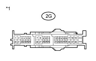
Text in Illustration *1 Front view of wire harness connector
(to Driver Side Junction Block Assembly)
Disconnect the 2G driver side junction block assembly connector.
-
Measure the resistance according to the value(s) in the table below.
Standard Resistance Tester Connection Condition Specified Condition 2G-10 - 2G-29 Ignition switch ON Below 1 Ω 2G-10 - 2G-9 Ignition switch ACC Below 1 Ω
NG
REPAIR OR REPLACE HARNESS OR CONNECTOR
OK
-
-
CHECK HARNESS AND CONNECTOR (DRIVER SIDE JUNCTION BLOCK ASSEMBLY - BODY GROUND)
-
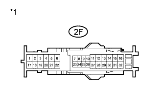
Text in Illustration *1 Front view of wire harness connector
(to Driver Side Junction Block Assembly)
Disconnect the 2F driver side junction block assembly connector.
-
Measure the resistance according to the value(s) in the table below.
Standard Resistance Tester Connection Condition Specified Condition 2F-16 - Body ground Always Below 1 Ω
NG
REPAIR OR REPLACE HARNESS OR CONNECTOR
OK
REPLACE MAIN BODY ECU (DRIVER SIDE JUNCTION BLOCK ASSEMBLY) Click here
-