CLOCK SYSTEM Power Source Circuit
DESCRIPTION
This circuit is the power source for the clock assembly. This circuit provides two types of power sources; one is a constant power source mainly used as a backup power source, and the other is a power source mainly used for signal transmission.
Tech Tips
If the clock assembly displays "1:00" when the ignition switch off, then on (IG) again, the B (*1) or +B (*2) terminal has a malfunction.
The maximum clock assembly margin of error is -4 to 4 seconds per day when the temperature is between -20°C (-4°F) and 60°C (140°F).
-
*1: w/o Multi-information Display
-
*2: w/ Multi-information Display
WIRING DIAGRAM
-
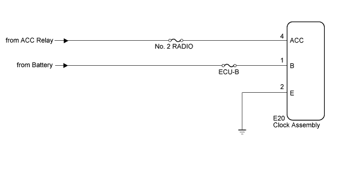
w/o Multi-information Display
-
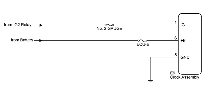
w/ Multi-information Display
INSPECTION PROCEDURE
PROCEDURE
-
CHECK HARNESS AND CONNECTOR
-
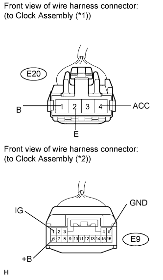
Disconnect the E20 (*1) or E9 (*2) connector.
-
Measure the voltage according to the value(s) in the table below.
Standard voltage Tester Connection Condition Specified Condition E20-1 (B) (*1) - Body ground Always 11 to 14 V E9-6 (+B) (*2) - Body ground Always 11 to 14 V E20-4 (ACC) (*1) - Body ground Ignition switch on (ACC) 11 to 14 V E9-1 (IG) (*2) - Body ground Ignition switch on (IG) 11 to 14 V *1: w/o Multi-information Display
*2: w/ Multi-information Display
-
Measure the resistance according to the value(s) in the table below.
Standard resistance Tester Connection Condition Specified Condition E20-2 (E) (*1) - Body ground Always Below 1 Ω E9-5 (GND) (*2) - Body ground Always Below 1 Ω *1: w/o Multi-information Display
*2: w/ Multi-information Display
Result Result Proceed to OK (w/o Multi-information Display) A OK (w/ Multi-information Display) B NG C
B 
REPLACE CLOCK ASSEMBLY (w/ Multi-information Display) Click here
C
REPAIR OR REPLACE HARNESS OR CONNECTOR
A 
REPLACE CLOCK ASSEMBLY (w/o Multi-information Display) Click here
-